


NEWS
CVD electric furnace (chemical vapor deposition furnace) can indeed process semiconductor materials. The following is a detailed explanation of CVD electric furnaces in semiconductor material processing:
")
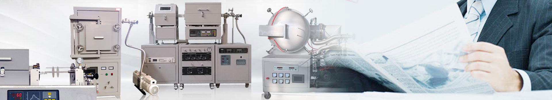
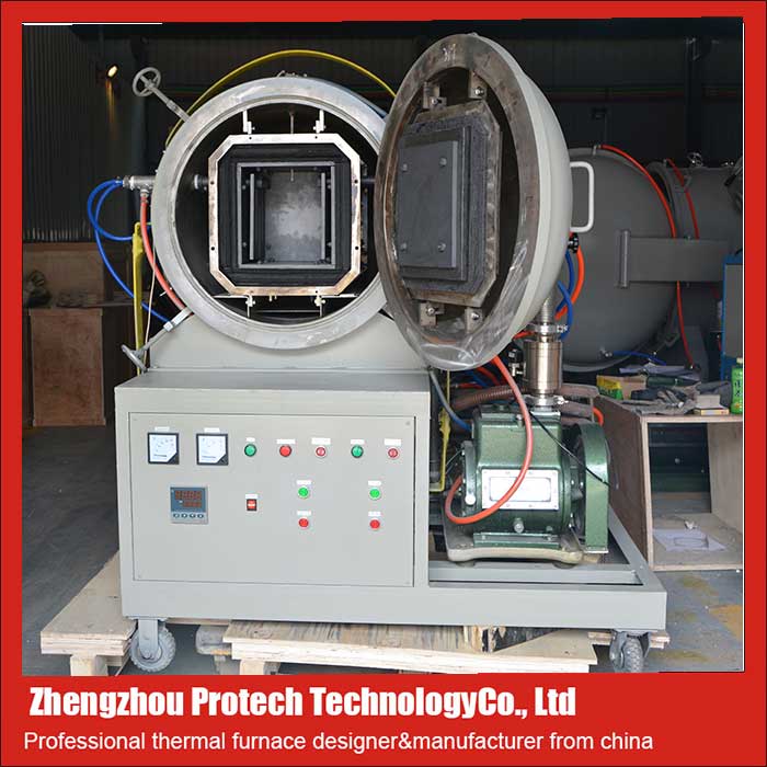
Commonly used CVD electric furnaces (click on the image to view product details)
1. The basic principle of CVD electric furnace
CVD electric furnace, also known as chemical vapor deposition electric furnace, is a heat treatment equipment that uses chemical reactions to deposit gas on a substrate to form the desired material. In the semiconductor industry, CVD electric furnaces are commonly used to decompose and deposit certain components on substrates (such as wafers) through chemical reactions between atoms and molecules of gaseous precursor reactants, forming thin films or other structures.
2. Application of CVD electric furnace in semiconductor material processing
Insulation layer deposition: CVD electric furnaces can be used to deposit insulation layers such as silicon dioxide (SiO ₂) and silicon nitride (Si ∝ N ₄), which serve as electrical insulation, protection, and passivation in semiconductor devices.
Metal layer deposition: deposition of metal layers such as tungsten (W), titanium (Ti), titanium nitride (TiN), and aluminum (Al), mainly used for interconnection and contact hole filling.
Doping layer deposition: such as the deposition of phosphosilicate glass (PSG) and borosilicate glass (BSG), used for local doping and surface passivation to improve the performance of semiconductor devices.
Epitaxial growth: CVD electric furnaces are also used for epitaxial growth of single crystal silicon or other semiconductor materials (such as silicon carbide and gallium nitride), forming high-quality single crystal layers on the wafer surface, which is important for improving the integration and performance of devices.
High k material deposition: deposition of high k dielectric materials such as hafnium oxide (HfO ₂) and zirconium oxide (ZrO ₂), which are used as MOSFET gate dielectrics to reduce leakage current and improve device performance.
Barrier layer deposition: deposition of titanium nitride (TiN) and tantalum nitride (TaN) as diffusion barriers for copper interconnects, preventing metal diffusion and protecting device integrity.
3. The advantages of CVD electric furnace in the semiconductor industry
High purity and high quality: CVD process can deposit high-purity and low defect thin films, ensuring device performance and reliability.
Uniformity and controllability: By precisely controlling the flow rate and reaction conditions of gas-phase reactants, the thickness and composition uniformity of the film can be achieved.
")
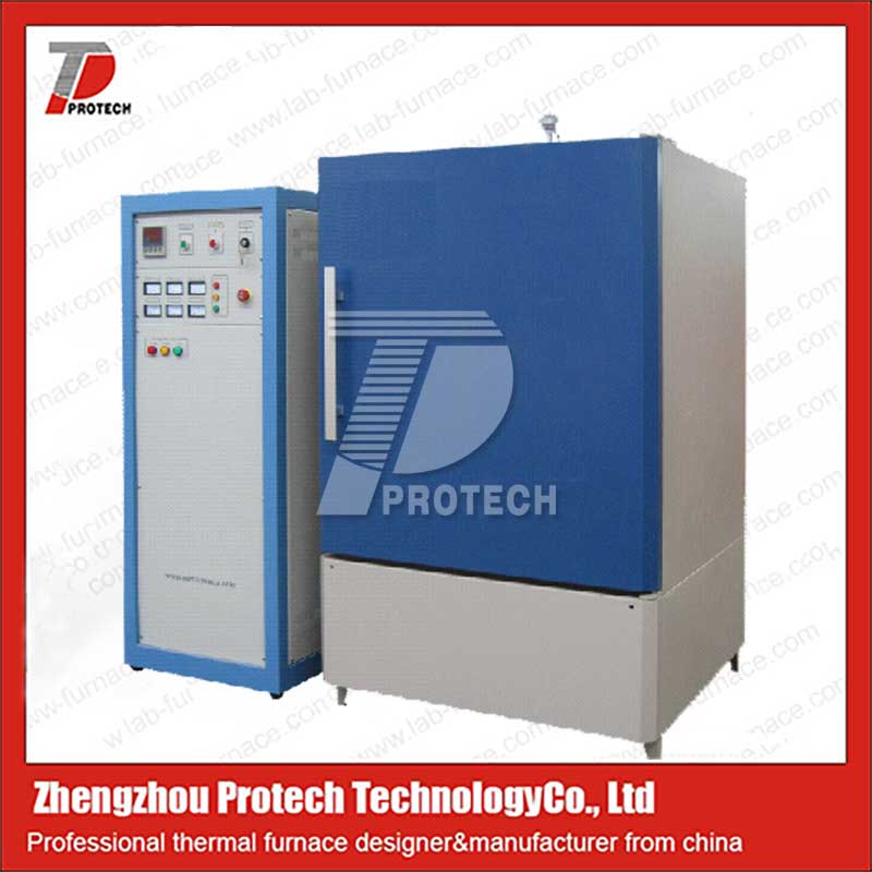
Customized sliding CVD electric furnace (click on the image to view product details)
So, CVD electric furnaces have a wide range of applications and significant advantages in semiconductor material processing. It is one of the important tools in the semiconductor manufacturing process.Click to learn more CVD devices! Or click on online customer service to learn more about product information!
Leave A Message


